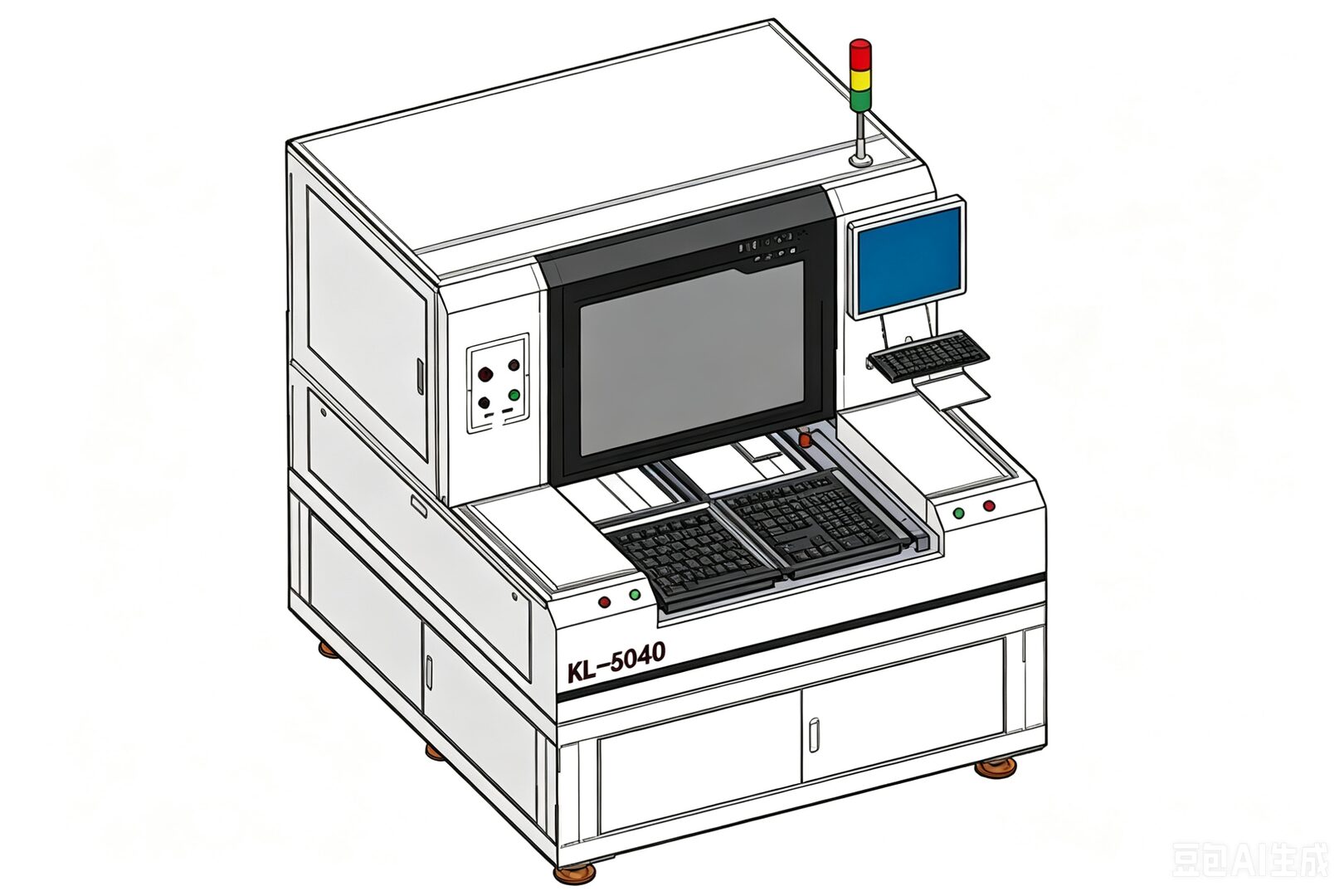
Precision single-station UV laser depaneling machine with cold processing technology. Non-contact cutting eliminates thermal stress, making it ideal for sensitive semiconductor and electronic components.
Single-Station Precision Design - Optimized for high-accuracy single-point operations with maximum stability
UV Cold Processing Technology - Zero thermal stress on sensitive semiconductor components
Non-Contact Zero Stress Cutting - No mechanical force on delicate electronic parts
CAD Import Function - Direct CAD file import for flexible programming
SCANLAB Precision Galvo - Imported galvo scanner for exceptional beam control
Precision Focus: Single-station design prioritizes accuracy over speed - ideal for high-value PCBs
Cold Processing Advantage: UV technology eliminates heat damage - perfect for sensitive components
30+ Years Expertise: Manufacturer with nearly three decades of PCB depaneling experience since 1995
| Parameter | Specification |
|---|---|
| Platform Moving Range | 450 × 550mm |
| Maximum Cutting Range | Length 550mm × Width 450mm |
| Platform Positioning Accuracy | ±3μm |
| Platform Repeat Positioning Accuracy | ±2μm |
| CCD Positioning Accuracy | <±5μm |
| Minimum Cutting Line Width | <15μm |
| Laser Output Power | 25W / 30W / 40W |
| Equipment Dimensions | 1750 × 1750 × 1700mm |
| Equipment Weight | Approx. 1850kg |
| Work Station Type | Single-Station Precision Cutting |
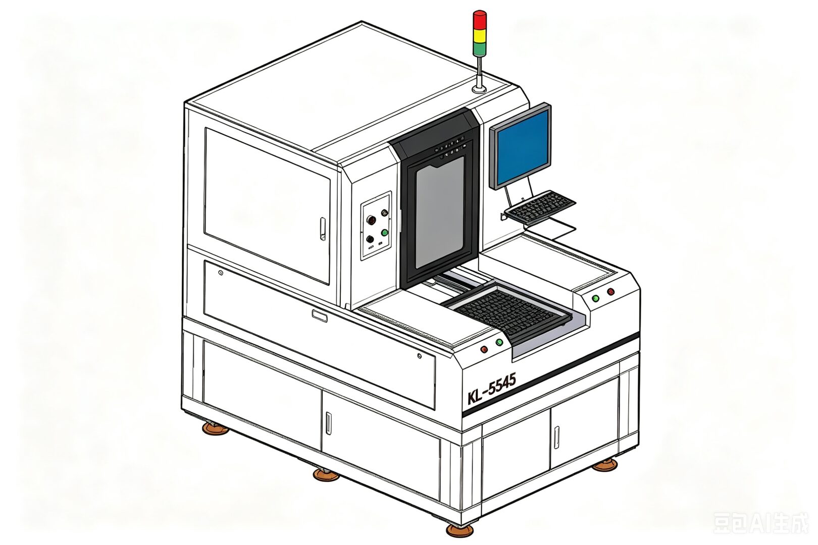
Single-Station Precision Design - Optimized for high-accuracy single-point operations
UV Cold Processing Technology - Zero thermal stress on sensitive components
Non-Contact Zero Stress Cutting - No mechanical force on delicate parts
CAD Import Function - Direct CAD file import for flexible programming
SCANLAB Precision Galvo - Imported galvo scanner for exceptional beam control
High-Speed Cutting - Efficient production with minimal heat affected zone
The KL-5545 features a platform moving range of 550×450mm with maximum cutting range of 550mm length × 450mm width. This single-station design provides excellent precision for medium-sized PCB panels.
UV cold processing uses ultraviolet laser energy to vaporize material without generating heat. This eliminates thermal stress on sensitive components, prevents warping or damage to temperature-sensitive materials, and produces cleaner cuts with no heat-affected zones.
The KL-5545 achieves ±3μm platform positioning accuracy and ±2μm repeat positioning accuracy. The CCD vision system provides positioning accuracy of less than ±5μm. Minimum cutting line width is less than 15μm.
The KL-5545 is ideal for semiconductor chip processing, FPC coating opening, appearance forming, and PCBA depaneling. Its non-contact cutting makes it perfect for sensitive electronic components.
The KL-5545 uses SCANLAB precision galvo scanner (imported) for exceptional beam positioning, INNO UV laser source (joint venture), and premium linear components. This ensures reliable, high-precision operation.
Contact our sales team for detailed specifications, pricing, and customized solutions tailored to your production requirements.
Get Your KL-5545 Quote Now